- 您现在的位置:买卖IC网 > Sheet目录368 > W25Q64DWZEIG (Winbond Electronics)IC FLASH SPI 64MBIT 8WSON
W25Q64DW
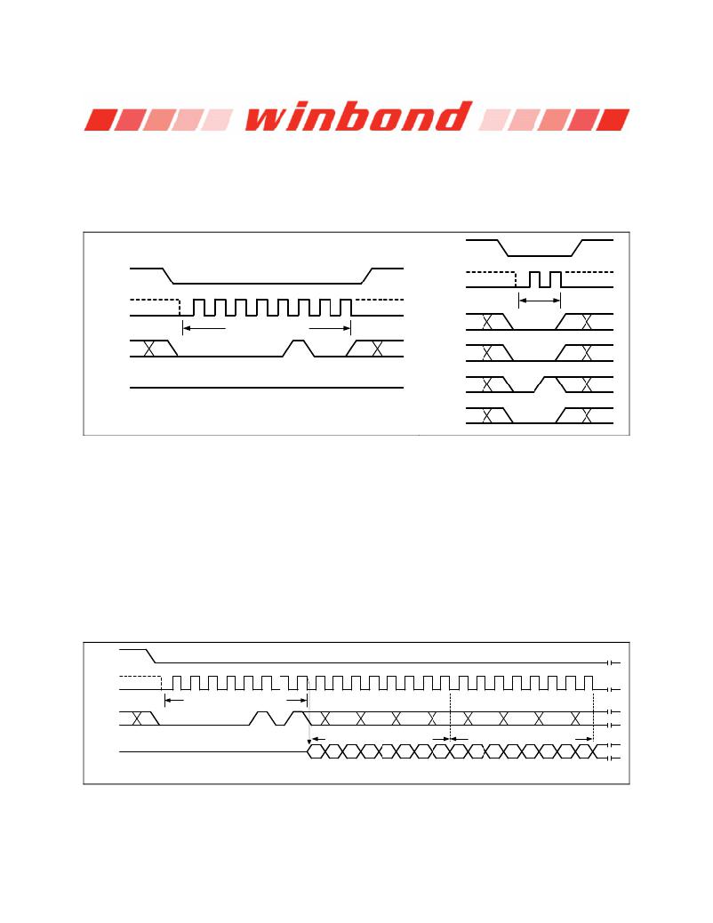
10.2.8 Write Disable (04h)
The Write Disable instruction (Figure 7) resets the Write Enable Latch (WEL) bit in the Status Register to
a 0. The Write Disable instruction is entered by driving /CS low, shifting the instruction code “04h” into the
DI pin and then driving /CS high. Note that the WEL bit is automatically reset after Power-up and upon
completion of the Write Status Register, Erase/Program Security Registers, Page Program, Quad Page
Program, Sector Erase, Block Erase, Chip Erase and Reset instructions.
/CS
/CS
CLK
Mode 3
Mode 0
0
1
Mode 3
Mode 0
Mode 3
0
1
2
3
4
5
6
7
Mode 3
In structio n
CLK
Mode 0
Mode 0
04h
DI
(IO 0 )
Instruction (04h)
IO 0
IO 1
DO
(IO 1 )
High Impedance
IO 2
IO 3
Figure 7. Write Disable Instruction for SPI Mode (left) or QPI Mode (right)
10.2.9 Read Status Register-1 (05h) and Read Status Register-2 (35h)
The Read Status Register instructions allow the 8-bit Status Registers to be read. The instruction is
entered by driving /CS low and shifting the instruction code “05h” for Status Register-1 or “35h” for
Status Register-2 into the DI pin on the rising edge of CLK. The status register bits are then shifted out on
the DO pin at the falling edge of CLK with most significant bit (MSB) first as shown in Figure 8. The Status
Register bits are shown in Figure 4a and 4b and include the BUSY, WEL, BP2-BP0, TB, SEC, SRP0,
SRP1, QE, LB3-0, CMP and SUS bits (see Status Register section earlier in this datasheet).
The Read Status Register instruction may be used at any time, even while a Program, Erase or Write
Status Register cycle is in progress. This allows the BUSY status bit to be checked to determine when the
cycle is complete and if the device can accept another instruction. The Status Register can be read
continuously, as shown in Figure 8. The instruction is completed by driving /CS high.
/CS
Mode 3
0
1
2
3
4
5
6
7
8
9
10
11
12
13
14
15
16
17
18
19
20
21
22
23
CLK
Mode 0
Instruction (05h or 35h)
DI
(IO 0 )
DO
(IO 1 )
*
= MSB
High Impedance
7
*
Status Register 1 or 2 out
6 5 4 3 2 1
0
7
*
Status Register 1 or 2 out
6 5 4 3 2 1
0
7
Figure 8a. Read Status Register Instruction (SPI Mode)
- 24 -
发布紧急采购,3分钟左右您将得到回复。
相关PDF资料
W25Q64FVSFIG
IC SPI FLASH 64MBIT 16SOIC
W25Q80BVSNIG
IC SPI FLASH 8MBIT 8SOIC
W25Q80BWSSIG
IC FLASH SPI 8MBIT 8SOIC
W25X40BVZPIG
IC SPI FLASH 4MBIT 8WSON
W25X64VZEIG
IC FLASH 64MBIT 75MHZ 8WSON
W25X80AVDAIZ
IC FLASH 16MBIT 100MHZ 8DIP
W29GL032CB7A
IC FLASH 32MBIT 70NS 48TFBGA
W29GL064CB7S
IC FLASH 64MBIT 70NS 48TSOP
相关代理商/技术参数
W25Q64DWZEIP
制造商:WINBOND 制造商全称:Winbond 功能描述:1.8V 64M-BIT SERIAL FLASH MEMORY WITH DUAL/QUAD SPI & QPI
W25Q64DWZPIG
功能描述:IC FLASH SPI 64MBIT 8WSON RoHS:是 类别:集成电路 (IC) >> 存储器 系列:SpiFlash® 标准包装:1 系列:- 格式 - 存储器:闪存 存储器类型:闪存 - NAND 存储容量:4G(256M x 16) 速度:- 接口:并联 电源电压:2.7 V ~ 3.6 V 工作温度:0°C ~ 70°C 封装/外壳:48-TFSOP(0.724",18.40mm 宽) 供应商设备封装:48-TSOP I 包装:Digi-Reel® 其它名称:557-1461-6
W25Q64DWZPIP
制造商:WINBOND 制造商全称:Winbond 功能描述:1.8V 64M-BIT SERIAL FLASH MEMORY WITH DUAL/QUAD SPI & QPI
W25Q64FVDAIG
制造商:WINBOND 制造商全称:Winbond 功能描述:3V 64M-BIT SERIAL FLASH MEMORY WITH DUAL/QUAD SPI & QPI
W25Q64FVDAIP
制造商:WINBOND 制造商全称:Winbond 功能描述:3V 64M-BIT SERIAL FLASH MEMORY WITH DUAL/QUAD SPI & QPI
W25Q64FVSFIG
功能描述:IC SPI FLASH 64MBIT 16SOIC RoHS:是 类别:集成电路 (IC) >> 存储器 系列:SpiFlash® 标准包装:72 系列:- 格式 - 存储器:RAM 存储器类型:SRAM - 同步 存储容量:4.5M(256K x 18) 速度:133MHz 接口:并联 电源电压:3.135 V ~ 3.465 V 工作温度:0°C ~ 70°C 封装/外壳:100-LQFP 供应商设备封装:100-TQFP(14x20) 包装:托盘
W25Q64FVSFIG TR
制造商:Winbond Electronics Corp 功能描述: 制造商:Winbond Electronics Corp 功能描述:IC FLASH 64MBIT 104MHZ 16SOIC
W25Q64FVSFIP
制造商:WINBOND 制造商全称:Winbond 功能描述:3V 64M-BIT SERIAL FLASH MEMORY WITH DUAL/QUAD SPI & QPI
